ZTL TECH is now Zintilon. We’ve updated our name and logo for a fresh start. Check Now

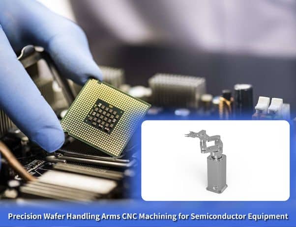
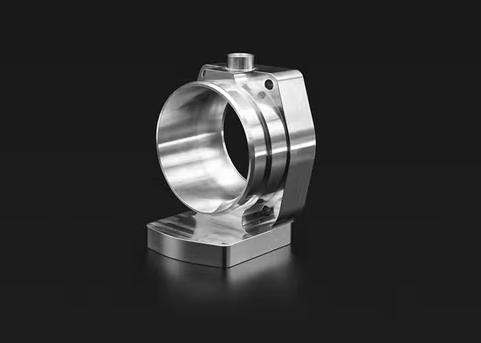
Precision Wafer Handling Arms CNC Machining for Semiconductor Equipment

Precision wafer handling arms are ultra-precise robotic components that transport silicon wafers between processing stations in semiconductor fabrication equipment. At Zintilon, we specialize in CNC machining of wafer handling arms using advanced multi-axis machining to achieve exceptional flatness, parallelism, and surface cleanliness for contamination-free wafer transfer and extended service life in cleanroom environments.
  • Machining for complex arm geometries and wafer contact surfaces
  • Tight tolerances up to ±0.0002 in
  • Ultra-precision milling, lapping & cleanroom-compatible finishing
  • Support for rapid prototyping and full-scale production
  • ISO 9001-certified semiconductor component manufacturing


Trusted by 15,000+ businesses

Why Semi-Conductor Companies
Choose Zintilon

prductivity

Increased Productivity

Engineers get time back by not dealing with immature supply chains or lack of supply chain staffing in their company and get parts fast.

10x

10x Tighter Tolerances

Zintilon can machine parts with tolerances as tight as+/ - 0.0001 in -10x greater precision compared to other leading services.

world

World Class Quality

Zintilon provides aerospace parts for leading aerospace enterprises, verified to be compliant with ISO9001 quality standard by a certified registrar. Also, our network includes AS9100 certified manufacturing partners, as needed.

From Prototyping to Mass Production

Zintilon provides CNC machining for precision wafer handling arms and related transfer components for semiconductor equipment manufacturers, wafer fab tool suppliers, and cleanroom automation companies worldwide.

Prototype Precision Wafer Handling Arm

Obtain high-precision prototypes of wafer handling arms that accurately replicate your final design. Test flatness, verify particle generation, and ensure contamination-free transfer before full-scale production.


Key Point

  • Rapid prototyping with ultra-precision

  • Tight tolerances (±0.0002 in)

  • Test design, cleanliness, and handling accuracy early

3 Axis CNC Machined Stainless Steel Passivation

EVT – Engineering Validation Test

Rapid iterating on wafer arm prototypes stands within the flatness and cleanliness requirements. Voice concerns early for seamless movement into full-scale semiconductor manufacturing.


Key Point

  • Validate prototype functionality

  • Rapid design iterations

  • Ensure readiness for production

Anodized Aluminum 1024x536

DVT – Design Validation Test

Assess the dimensional accuracy and the surfaces quality of the arms for handling wafers in different materials, and the design for optimal contamination control surfaces of the arms before the mass production.


Key Point

  • Confirm design integrity and flatness

  • Test multiple materials and surface treatments

  • Ensure production-ready performance

design aluminium

PVT – Production Validation Test

Check large-scale production for the arms, and the potential full production hoarding to identify the production of secured manufacturing for the arm handles.


Key Point

  • Test large-scale production capability

  • Detect and fix process issues early

  • Ensure consistent part quality

Anodized Titanium Fastener

Mass Production

Rapidly manufacture high quality, cleanroom-grade, and contamination-free operational wafer handling arms to ensure timely delivery to semiconductor equipment manufacturers and wafer fabrication facilities.


Key Point

  • Consistent, high-volume production

  • Ultra-precision machining for cleanroom quality

  • Fast turnaround with strict quality control

production

Simplified Sourcing for
the New Energy Industry

Our aviation industry parts manufacturing capabilities have been verified by many listed companies. We provide a variety of manufacturing processes and surface treatments for aerospace parts including titanium alloys and aluminum alloys.

Explore Other Semiconductor Components

Browse our complete selection of CNC machined semiconductor components, crafted for durability and ultra-tight tolerances. From precision tooling and fixture parts to vacuum chambers and wafer handling systems, we deliver solutions tailored to advanced semiconductor production.

Semiconductor Precision Wafer Handling Arms Machining Capabilities

Our ultra-precision CNC machining centers and cleanroom facilities equipped with dedicated semiconductor machinists enables us to CNC Machine Precision Wafer Handling Arms for Semiconductor Equipment. From end effector blades to multi-arm assemblies and vacuum pads, we precisely machine and meet critical flatness specifications for every component, ensuring optimal wafer support, minimizing particle generation, and ensuring contamination-free operation during wafer handling.

Ultra-precision milling, lapping, electropolishing, and cleanroom assembly via flattening laser interferometry and particle control enables us to design wafer contact surfaces with extreme flatness. We also perform particle control for surfaces of wafer handling arms to meet required specifications. We machine wafer handling arms from aluminum alloys (6061-T6, 7075-T6), ceramics (alumina, silicon carbide), and composite materials (carbon fiber), which ensure high rigidity and low outgassing during vacuum in semiconductor processing.
milling

CNC Machining

sheet metal

Sheet Metal Fabrication

edm

Wire EDM

casting

Metal Casting

Aerospace
Materials & Finishes

Materials
We provide a wide range of materials, including metals, plastics, and composites.
Finishes
We offer superior surface finishes that enhance part durability and aesthetics for applications requiring smooth or textured surfaces.

Specialist Industries

you are welcome to emphasize it in the drawings or communicate with the sales.

Materials for Precision Wafer Handling Arms

For Wafer Handling Arms Machining for Semiconductor Equipment, our CNC machine shop provides a wide range of materials. It comprises 12+ cleanroom-compatible metals as well as a variety of ceramics and composites, ensuring rapid prototyping and ultra-precision semiconductor component fabrication with consistent quality and contamination control.
Aluminum Image

High machinability and ductility. Aluminum alloys have good strength-to-weight ratio, high thermal and electrical conductivity, low density and natural corrosion resistance.

Price
$ $ $
Lead Time
< 7 days
Tolerances
Down to ±0.003 mm
Max part size
3000*2200*1100 mm
Min part size
2*2*2 mm
Steel Image

Steel is a strong, versatile, and durable alloy of iron and carbon. Steel is strong and durable. High tensile strength, corrosion resistance heat and fire resistance, easily molded and formed. Its applications range from construction materials and structural components to automotive and aerospace components.

Price
$ $ $ $ $
Lead Time
< 10 days
Tolerances
Down to ±0.001 mm (routing)
Max part size
3000*2200*1100 mm
Min part size
2*2*2 mm
Stainless steel Image

Stainless steel alloys have high strength, ductility, wear and corrosion resistance. They can be easily welded, machined and polished. The hardness and the cost of stainless steel is higher than that of aluminum alloy.

Price
$ $ $
Lead Time
< 7 days
Tolerances
Down to ±0.005 mm
Max part size
3000*2200*1100 mm
Min part size
2*2*2 mm
Titanium Image

Titanium is an advanced material with excellent corrosion resistance, biocompatibility, and strength-to-weight characteristics. This unique range of properties makes it an ideal choice for many of the engineering challenges faced by the medical, energy, chemical processing, and aerospace industries.

Price
$$$
Lead Time
< 10 days
Tolerances
Down to ±0.005 mm
Max part size
3000*2200*1100 mm
Min part size
2*2*2 mm
Bronze Image

Highly resistant to seawater corrosion. The material’s mechanical properties are inferior to many other machinable metals, making it best for low-stress components produced by CNC machining.

Price
$ $ $ $ $
Lead Time
< 10 days
Tolerances
Down to ±0.005 mm
Max part size
3000*2200*1100 mm
Min part size
2*2*2 mm
Brass Image

Brass is mechanically stronger and lower-friction metal properties make CNC machining brass ideal for mechanical applications that also require corrosion resistance such as those encountered in the marine industry.

Price
$$$
Lead Time
< 10 days
Tolerances
Down to ±0.005mm
Max part size
3000*2200*1100 mm
Min part size
2*2*2 mm
Copper Image

Few metals have the electric conductivity that copper has when it comes to CNC milling materials. The material’s high corrosion resistance aids in preventing rust, and its thermal conductivity features facilitate CNC machining shaping.

Price
$$$
Lead Time
< 10 days
Tolerances
Down to ±0.005 mm
Max part size
3000*2200*1100 mm
Min part size
2*2*2 mm
Magnesium Image

Due to the low mechanical strength of pure magnesium, magnesium alloys are mainly used. Magnesium alloy has low density but high strength and good rigidity. Good toughness and strong shock absorption. Low heat capacity, fast solidification speed, and good die-casting performance.

Price
$ $ $ $
Lead Time
< 7 days
Tolerances
Down to ±0.005 mm
Max part size
3000*2200*1100 mm
Min part size
2*2*2 mm
Iron Image

Iron is an indispensable metal in the industrial sector. Iron is alloyed with a small amount of carbon – steel, which is not easily demagnetized after magnetization and is an excellent hard magnetic material, as well as an important industrial material, and is also used as the main raw material for artificial magnetism.

Price
$ $ $ $ $
Lead Time
< 10 days
Tolerances
Down to ±0.005 mm
Max part size
3000*2200*1100 mm
Min part size
2*2*2 mm
Zinc Image

Zinc is a slightly brittle metal at room temperature and has a shiny-greyish appearance when oxidation is removed.

Price
$ $ $ $ $
Lead Time
< 10 days
Tolerances
Down to ±0.005 mm
Max part size
3000*2200*1100 mm
Min part size
2*2*2 mm
Let’s Build Something Great, Together

FAQs: Materials for Precision Wafer Handling Arms

Precision wafer handling arms are robotic components transporting silicon wafers measuring 200mm, 300mm, or 450mm diameter between processing chambers in fabrication equipment. Types include end effector blades with vacuum or mechanical edge gripping, dual-arm systems handling two wafers simultaneously for higher throughput, atmospheric transfer arms for non-vacuum environments, vacuum-compatible arms with low outgassing materials, extended-reach arms for cluster tool configurations, rotational arms with theta-axis motion, and specialty arms including backside contact designs, compliant edge grippers accommodating wafer thickness variation, and cryogenic-compatible arms for low-temperature processing stations.

Aluminum alloys 6061-T6 and 7075-T6 construction is lightweight which lowers inertia for high-speed motion and accelerations greater than 3 meters per second squared, also keeping stiffness so deflection does not exceed 0.05 millimeters under the weight of the wafer, machining complex geometries becomes easy, and the outgassing rates are acceptable and below 10^-8 Torr-liters per second per square centimeter in a vacuum environment. Ceramics such as alumina and silicon carbide provide the maximum stiffness to not allow the wafer to sag, ultra-low particle generation of less than 0.1 particles per square centimeter per wafer pass, outstanding flatness retention through temperature cycling, chemical resistance to plasmas and etchants, and ultra-high vacuum compatibility. Carbon fiber composites are the ultimate in weight reduction, and have 50 percent higher weight reduction than aluminum, have adequate stiffness, low thermal expansion to silicon wafer, and properties that can be tailored through fiber orientation.

Ultra-precision multi-axis CNC milling creates arm profiles with integrated, stiffening ribs, vacuum channels, and mounting interfaces. Precision lapping achieves wafer contact surface flatness of 0.0002 inches and parallelism of 0.0005 inches over a 300 mm span. Surface grinding produces flat reference surfaces. Coordinate drilling creates vacuum port patterns with position accuracy to ±0.002 inches. For ceramic arms, diamond machining produces finished surfaces. Electropolishing on aluminum to Ra < 0.2 microns minimizes particle adhesion sites. All final operations were performed in ISO Class 5 or better cleanrooms.

We achieve parallelism within 0.0005 inches between dual contact surfaces, vacuum port positions within ± 0.002 inches for consistent holding force distribution, surface finish of lapped surfaces to 0.2 Ra microns, straightness within 0.0005 inches per foot, and overall arm dimensions to ± 0.010 inches for robot integration.

Certainly! We provide rapid prototyping for semiconductor tools and conduct flatness and particle testing in ISO Class 5 cleanrooms. We also do low-volume production for custom process equipment where we do 10 to 200 arms, and we do medium-volume production for commercial wafer handling systems where we do hundreds to thousands of arms each year. We also offer complete bounded dimension checks using coordinate measuring machines, flatness checks using laser interferometry within 0.5 microns, particle generation testing following SEMI standards, outgassing measurements for vacuum compatibility, and material certifications. These include contamination and out gassing measurements.

Yes! We manufacture all components under an ISO 9001 quality management system which provides complete traceability of all materials. Components are verified against design specs for dimensions, documented flatness and parallelism measurements, particle generation testing per SEMI E52 standards, outgassing validation for vacuum applications, and beyond SEMI standards for contamination-free wafer handling. We also positioned the system to within 0.1 millimeters, and it has over 1 million wafer transfer cycles which exceeds the life expectation of the system.

These finishes encompass lapping to precision of Ra < 0.2 microns, lapping to a tolerance of 0.0002 inches flatness for wafer contact surfaces, and electropolishing on aluminum to a depth of 10 to 50 microns which eases surface s and smoothed edges to reduce adhesion of particles. Also, hard anodizing type II to a thickness of 25 to 50 microns for wear resistance while anodizing, dimensional tolerances are preserved. Other finishes are controlled bead blasting of non-contact surfaces. Specialized treatments devoid of organic impoverishment by plasma cleaning to sub 10^13 atoms/cm^2 and vapor honing for ultra-smooth cosmetic finishing.

Standard aluminum end effector arms require 15 to 20 business days which includes ultra-precision machining, lapping, and cleanroom processes. On the other hand, ceramic or composite arms of complex geometries would require 6 to 8 weeks. Particle testing prototype arms are built in 10 to 14 days which allows fast qualification and development of semiconductor tools.

The answer is yes. We create extended-reach arms for cluster tools with arm lengths over 600 millimeters and maintain a deflection of less than 0.05 millimeters. We also make high-temperature arms for thermal processing up to 400 degrees Celsius using ceramic construction, ultra high vacuum compatible arms whose outgassing rates are below 10^-9 Torr-liters per second, and multi-wafer handling arms that transfer 2 to 4 wafers at a time. We design compliant grippers that are able to accommodate and handle wafers that bow over 200 microns. We create contamination-resistant arms for use in wet processes and also design cryogenic arms for sub-zero processing, plasma-resistant arms for etch chambers, and metrology-grade arms for dimensional measurement systems that require positioning repeatability of 10 microns.

Fine contact surfaces that are level within 0.0002 inches results in perfectly even support, preventing wafer stresses that lead to crystalline defects and reduce the yield of the devices. Spaced parallel dual contact surfaces within 0.0005 inches results in the consistent spacing of the wafers, preventing collisions during the transfer of the wafers and ensuring the proper thermal contact during the processing in the chambers. Ultra-smooth surfaces, with a Roughness Average value of lower than 0.2 microns results in the minimization of particle adhesion sites, and thus the mitigation of surface contamination of the wafer, where single particles could lead to the failure of a device, of advanced nodes under 7nm. Proper arm stiffness prevents deflection more than 0.05mm, under the weight of the wafer… thus maintaining the required positioning accuracy of 0.1mm for automatic wafer centering. Low outgassing materials allow for vacuum pressures below 10^-7 Torr that inhibit contamination for the deposition and etch processes. Well designed vacuum ports give consistent lateral freely hinged wafer retention that prevents slippage of the wafer during high acceleration of more than 2g. Particle adder counts of below 0.1 particles per pass, positioning repeatability of within 0.05mm and over 1 million transfer cycles during years of continuous operation in 200mm, 300mm and the new, 450mm wafer fabs represent reliable wafer transfer.
Got any more questions?