ZTL TECH is now Zintilon. We’ve updated our name and logo for a fresh start. Check Now

Alignment Fixtures CNC Machining for Semiconductor Manufacturing

Alignment fixtures in semiconductor manufacturing are precision tools that help in accurately positioning components, orienting wafers, and calibrating tools during all phases of fabrication. At Zintilon, we focus on CNC machining of alignment jigs, reference fixtures, and calibration standards to ensure high repeatability, dimensional stability, and operational reliability in cleanroom production environments, all of which are critical for semiconductor manufacturing.
  • Machining for precision alignment features and reference surfaces
  • Tight tolerances up to ±0.0005 in for positioning accuracy
  • Precision milling, grinding & repeatability control
  • Support for rapid prototyping and full-scale production
  • ISO 9001-certified manufacturing with semiconductor industry expertise


Trusted by 15,000+ businesses

Why Semi-Concductor Companies
Choose Zintilon

prductivity

Increased Productivity

Engineers get time back by not dealing with immature supply chains or lack of supply chain staffing in their company and get parts fast.

10x

10x Tighter Tolerances

Zintilon can machine parts with tolerances as tight as+/ - 0.0001 in -10x greater precision compared to other leading services.

world

World Class Quality

Zintilon provides medical parts for leading aerospace enterprises, verified to be compliant with ISO9001 quality standard by a certified registrar.

From Prototyping to Mass Production

Zintilon offers CNC machining for alignment fixtures and other positioning apparatus to semiconductor equipment manufacturers, semiconductor fabrication tool suppliers, and process integration to manufacturing teams globally.

Prototype Alignment Fixtures Components

High precision prototype alignment fixture assemblies designed to your exact specifications are available for you to test. Ensure that all specifications for positioning repeatability, reference accuracy, and cleanroom are fully satisfied before moving on to semiconductor production at full scale.


Key Point

  • Rapid prototyping with high precision

  • Tight tolerances (±0.0005 in)

  • Test design, repeatability, and contamination control early

3 Axis CNC Machined Stainless Steel Passivation

EVT – Engineering Validation Test

Iterate rapidly on alignment fixture prototypes to finalize requirements for all positioning and processing. Anticipate issues in sequencing to facilitate transition to fully integrated semiconductor tooling capital equipment manufacturing.


Key Point

  • Validate prototype functionality

  • Rapid design iterations

  • Ensure readiness for production

Anodized Aluminum 1024x536

DVT – Design Validation Test

Test alignment fixture design for repeatability and accuracy performance, using different materials and reference configurations, to demonstrate design intent and positioning precision for mass production.


Key Point

  • Confirm design integrity and repeatability quality

  • Test multiple materials and configurations

  • Ensure production-ready performance

design aluminium

PVT – Production Validation Test

Assess alignment fixture mass production to verify intended objectives are confirmed, and identify production control points and feasible mitigation strategies to meet defined objectives before production begins.


Key Point

  • Test large-scale production capability

  • Detect and fix process issues early

  • Ensure consistent part quality

finishes

Mass Production

High quality, alignment fixture production at semiconductor processing tolerances, and precise and accurate positioning to ensure on-time delivery to fabricating equipment manufacturers and manufacturing processing tool suppliers.


Key Point

  • Consistent, high-volume production

  • Precision machining for semiconductor-grade quality

  • Fast turnaround with strict quality control

production

Simplified Sourcing for
Robotics Industry

Our robotics industry parts manufacturing capabilities have been verified by many listed companies. We provide a variety of manufacturing processes and surface treatments for robotics parts including titanium alloys and aluminum alloys.

Explore Other Semiconductor Components

Browse our complete selection of CNC machined semiconductor components, crafted for durability and ultra-tight tolerances. From precision tooling and fixture parts to vacuum chambers and wafer handling systems, we deliver solutions tailored to advanced semiconductor production.

Semiconductor Manufacturing Alignment Fixtures Machining Capabilities

Equipped with CNC multi-axis machining centers and precision grinding tools coupled with CMM verification tools, along with numerous seasoned semiconductor tooling machinists, Alignment Fixtures CNC Machining for Semiconductor Manufacturing is achieved. Components, from wafer alignment jigs to die bonding fixtures and metrology reference standards with precision locating features, are engineered for advanced semiconductor fabrication and assembly processes to achieve submicron repeatability, minimal thermal drift, and cleanroom compliance.

For precision CNC milling, surface grinding for reference flatness, and EDM for intricate features, dimensional stabilization treatments, followed by CMM inspection, and gauge R&R validation are provided. Alignment fixtures are machined from aluminum alloys, stainless steel, tool steel, or technical ceramics to provide high dimensional stability, wear resistance, and particle-free operation in continuous use within a semiconductor cleanroom environment.
milling

CNC Machining

sheet metal

Sheet Metal Fabrication

edm

Wire EDM

casting

Metal Casting

Aerospace
Materials & Finishes

Materials
We provide a wide range of materials, including metals, plastics, and composites.
Finishes
We offer superior surface finishes that enhance part durability and aesthetics for applications requiring smooth or textured surfaces.

Specialist Industries

you are welcome to emphasize it in the drawings or communicate with the sales.

Materials for Alignment Fixtures Components

Our CNC machine shop provides various Alignment Fixtures Machining for Semiconductor Manufacturing materials. We have over 15 precision materials and cleanroom-compatible alloys. For rapid prototyping and precision semiconductor tooling manufacturing, we maintain quality and fab-grade material specifications for all semiconductors..
Aluminum Image

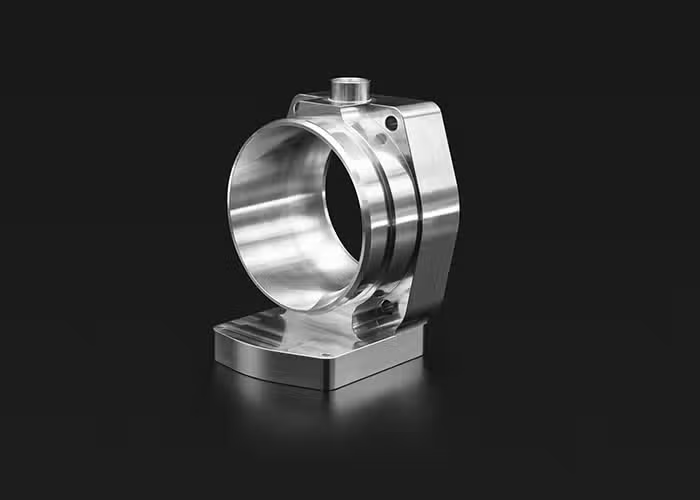
High machinability and ductility. Aluminum alloys have good strength-to-weight ratio, high thermal and electrical conductivity, low density and natural corrosion resistance.
Price
$ $ $
Lead Time
< 7 days
Tolerances
Down to ±0.003 mm
Max part size
3000*2200*1100 mm
Min part size
2*2*2 mm
Stainless steel Image

Stainless steel alloys have high strength, ductility, wear and corrosion resistance. They can be easily welded, machined and polished. The hardness and the cost of stainless steel is higher than that of aluminum alloy.

Price
$ $ $
Lead Time
< 7 days
Tolerances
Down to ±0.005 mm
Max part size
3000*2200*1100 mm
Min part size
2*2*2 mm
Titanium Image

Titanium is an advanced material with excellent corrosion resistance, biocompatibility, and strength-to-weight characteristics. This unique range of properties makes it an ideal choice for many of the engineering challenges faced by the medical, energy, chemical processing, and aerospace industries.

Price
$$$
Lead Time
< 10 days
Tolerances
Down to ±0.005 mm
Max part size
3000*2200*1100 mm
Min part size
2*2*2 mm
Steel Image

Steel is a strong, versatile, and durable alloy of iron and carbon. Steel is strong and durable. High tensile strength, corrosion resistance heat and fire resistance, easily molded and formed. Its applications range from construction materials and structural components to automotive and aerospace components.

Price
$ $ $ $ $
Lead Time
< 10 days
Tolerances
Down to ±0.001 mm (routing)
Max part size
3000*2200*1100 mm
Min part size
2*2*2 mm
Bronze Image

Highly resistant to seawater corrosion. The material’s mechanical properties are inferior to many other machinable metals, making it best for low-stress components produced by CNC machining.

Price
$ $ $ $ $
Lead Time
< 10 days
Tolerances
Down to ±0.005 mm
Max part size
3000*2200*1100 mm
Min part size
2*2*2 mm
Copper Image

Few metals have the electric conductivity that copper has when it comes to CNC milling materials. The material’s high corrosion resistance aids in preventing rust, and its thermal conductivity features facilitate CNC machining shaping.

Price
$$$
Lead Time
< 10 days
Tolerances
Down to ±0.005 mm
Max part size
3000*2200*1100 mm
Min part size
2*2*2 mm
Brass Image

Brass is mechanically stronger and lower-friction metal properties make CNC machining brass ideal for mechanical applications that also require corrosion resistance such as those encountered in the marine industry.

Price
$$$
Lead Time
< 10 days
Tolerances
Down to ±0.005mm
Max part size
3000*2200*1100 mm
Min part size
2*2*2 mm
Zinc Image

Zinc is a slightly brittle metal at room temperature and has a shiny-greyish appearance when oxidation is removed.

Price
$ $ $ $ $
Lead Time
< 10 days
Tolerances
Down to ±0.005 mm
Max part size
3000*2200*1100 mm
Min part size
2*2*2 mm
Iron Image

Iron is an indispensable metal in the industrial sector. Iron is alloyed with a small amount of carbon – steel, which is not easily demagnetized after magnetization and is an excellent hard magnetic material, as well as an important industrial material, and is also used as the main raw material for artificial magnetism.
Price
$ $ $ $ $
Lead Time
< 10 days
Tolerances
Down to ±0.005 mm
Max part size
3000*2200*1100 mm
Min part size
2*2*2 mm
Magnesium Image

Due to the low mechanical strength of pure magnesium, magnesium alloys are mainly used. Magnesium alloy has low density but high strength and good rigidity. Good toughness and strong shock absorption. Low heat capacity, fast solidification speed, and good die-casting performance.

Price
$ $ $ $
Lead Time
< 7 days
Tolerances
Down to ±0.005 mm
Max part size
3000*2200*1100 mm
Min part size
2*2*2 mm
Let’s Build Something Great, Together

FAQs: Alignment Fixtures for Semiconductor Manufacturing Applications

Alignment fixtures are tools that position and align components precisely and calibrate devices for all semiconductor manufacturing processes. Alignment fixtures come in many forms, including wafer alignment jigs that position substrates for lithography and metrology tools, die bonding fixtures that maintain submicron placement accuracy for chip assembly, reticle alignment frames that control photomask orientation, gauge blocks and reference standards for equipment calibration, assembly fixtures for flip-chip and wire bonding, and inspection fixtures that verify dimensions. Test socket alignment plates for end-of-line testing and specialty fixtures like notch finders for wafer orientation are also alignment fixtures. Other alignment fixtures include mechanical datums for coordinate reference and kinematic mounting bases that provide repeatable positioning within 1 micron for wafer handling, device assembly, and quality control operations.

Aluminum grades 6061-T6, 7075-T6, and MIC-6, as well as the previously listed lightweight, minimally dimensionally changing, and low internal stress, manufacturably sophisticated, and thermally conductive grades, for reducing gradients, also possess thermally induced gradients, and lightweight construction features, and generate low particles after appropriate surface finishing, are highly advantageous for the construction of specialized locating mechanical components and are dimensional appropriate for alignment fixture components of lower weight construction. Stainless steels of the grades 304, 316, and 17-4 PH, in a cleaning environment as a constituent of a cleaning chemically employed, as well as in cleaning environment process gases, are respected for non-magnet as well as respectively secures corrosion community and dominant of sensitive measure environment, appropriate geometry preserving stiffness, and clean room compatibility. Tool steels of the grades D2 and A2, in contrarily dimensional stability as well as after heat treatment and precision grindability, unimpaired surface interaction of locating surfaces, as well as maintaining wear resistance and high hardness fixed the rate of wear, at, over 1 million contact cycle, and respectively the encompassing contact surface exceeding cycle, locating surface, are favored for alignment fixture.

The intricacies of milling fixtures are executed using 5-axis CNC milling for the creation of locating pins, vacuum channels, and nesting components while maintaining a tolerance of +/- 0.0005 inches. Surface grinding completes the referenced surface grinding for flatness within 0.001 inches and parallelism within 0.0005 inches. After completing the precision drilling, locating hole patterns are acquired, and positional accuracy is achieved within +/- 0.0002 inches. Relief features and thin slots are designed using EDM. Cylindrical grinding guarantees the production of precision pins while maintaining a tolerance of +/- 0.0001 inches on the diameter. For slip-fit and press-fit assemblies, the required bore is reached during the honing process. Heat treatment regulating stress and hardening of the fixture guarantees the required dimensions and wear resistance.

Locating features with a tolerance of +/- 0.0005 inches are achieved for the repeatability of submicron placement of components, surface grinding ensures flatness of 0.001 inches for stable datum planes, hole diameter tolerances of +/- 0.0001 inches are achieved for precision pin fits, perpendicularity and parallelism of 0.0005 inches is achieved between mounting surfaces and between fixture halves respectively, a surface finish of 0.8 Ra microns is attained on mating surfaces, alignment fixtures in semi-conductor mounting systems for handling 200mm and 300mm wafers. The accuracy of die placement is within 5 microns with a measurement repeatability of 1 micron.

Yes, we provide rapid prototyping to verify fit and test assembly, with same-day CAD-to-part capability available for critical projects. For custom automation cells and research platforms, we perform low-volume production of 20 to 500 brackets. For standardized robot models, we perform high-volume production of thousands to tens of thousands of brackets annually, incorporating complete dimensional inspection, flatness verification, and material certifications.

All alignment fixtures can be certified and traceability can be demonstrated. All components are manufactured under ISO 9001 certified quality management systems with cleanroom assembly protocols where required, complete material traceability including composition certificates and thermal expansion data, dimensional verification using calibrated CMM equipment to NIST standards, repeatability validation through gauge R&R studies achieving GR&R below 10 percent, and adherence to semiconductor industry requirements including SEMI standards for materials and cleanliness, dimensional stability specifications, ESD protection per ANSI/ESD S20.20 for electronic component handling, and cleanroom compatibility per ISO 14644 Class 1 to Class 1000 requirements.

We provide comprehensive finishing solutions tailored to aerospace requirements:
Anodizing (Type II and Type III)
Passivation for corrosion resistance
Precision polishing for aerodynamic surfaces
Custom protective coatings and thermal barriers

Standard alignment fixtures from established designs require 12–18 business days including machining, heat treatment where required, surface finishing, and dimensional verification, while complex custom fixture assemblies with integrated sensors and multi-component nests need 4–6 weeks. Prototype alignment fixtures for process validation can be completed in 8–12 days depending on material availability and heat treatment requirements.

Yes. We create alignment fixtures for specific wafer sizes, including 200mm, 300mm, and 450mm. We also make high-temperature fixtures for thermal processing up to 400 degrees Celsius using Invar and ceramic materials. We design vacuum fixtures for load lock and process chambers with outgassing rates below 10⁻⁸ torr-L/s. We make compound semiconductor fixtures for GaAs, GaN, and SiC. We also make thin wafer fixtures for supporting substrates under 100 microns, multi-die gang bonding fixtures for simultaneous assembly, kinematic coupling fixtures for repeatable positioning to 0.5 microns, and other integrated systems for flexible manufacturing such as automated fixture changers, sensor-based smart fixtures, and modular nest systems.

The repeatability of the positioning of components is within 5 microns, which is less than ±0.0005 inch locating feature positions . This repeatability is sufficient for accurate die bonding and flip-chip assemblies, which is critical for meeting the specified overlay. The flatness of the reference surfaces is controlled within 0.001 inch, which aids in planar datum stability and measurement accuracy, and also aids in preventing the workpiece from distorting during processing. Patterns of holes are made accurately, which gives the required penn placement for slip fits that have clearances of 1 to 3 microns, which aids in repeatable component locating. Wear from 1, 000, 000 plus contact cycles does not cause positioning drift. This is due to the high surface hardness from thermal treatment of the locating surfaces. The ± 0.0005 inch perpendicularity tolerance avoids tilt errors due to improper component orientation. The thermal stability of the fixture materials, especially the precision crafted ones, control the geometry of the fixtures within 2 microns, despite 20 to 25 degree Celsius temperatures in fab environments. This is temperature variation. The surface finishes being better than 0.8 Ra microns ensure that particle generation is within the requirements for a Class 10 cleanroom, which is particle counts of less than 10 per 0.1 cubic foot. The alignment of the semiconductors becomes more reliable due to precision manufacturing. This aids in processing the wafer, assembling the devices, and inspecting the quality which is based on repeatability of positioning at a submicron level. This also involves stability of measurement for several years, controlled dimensional drift, contamination, and process capability indices (Cpk) of critical measurements and placement operations in high volume semiconductor manufacturing which is greater than 1.67.
Got any more questions?