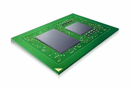
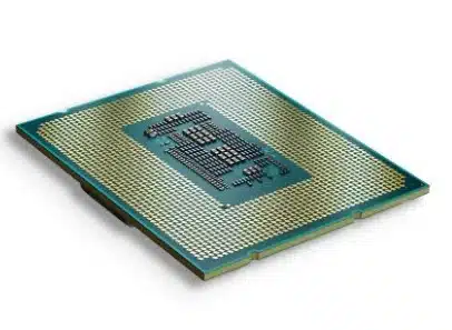
ZTL TECH is now Zintilon. We’ve updated our name and logo for a fresh start. Check Now

FC PCB Assembly

FC PCB Assembly refers to a board-level assembly service that centers on Flip-Chip technology. It involves directly soldering the electrical side of the chip face-down onto the substrate pads, supplemented by processes such as underfilling, laser ball placement, and BGA packaging. This technology achieves "the shortest interconnection, the lowest parasitics, and the highest density".
  • Maximum panel size 54 inches
  • Maximum panel thickness 0.450 inches

Start a new PCB Quote

FC PCB Assembly parts prototypes

Please compress all .gbr files before uploading
All uploads are secure and confidential

Our FC PCB Assembly Service Capabilities

Zintilon Technology is committed to providing advanced FC PCB assembly services to global users, supporting FC PCB assembly from prototype production in the product R&D stage to small-batch manufacturing. From printing to assembly, we ensure to deliver efficient and reliable FC PCB assembly solutions for you.
FC BGA

FC-BGA

FC CSP

FC-CSP

FC LGA

FC-LGA

FC PCB Assembly Materials

LayerRecommended Model/SpecificationKey ParametersRemarks
Chip BumpHigh-lead 95Pb5Sn (C4) or SAC305 micro-bumpDiameter: 60–100 µm; Height: 50–80 µm; Pitch: 80–150 µmHigh-lead bumps have a melting point of 320°C and can withstand high temperatures in subsequent processes; lead-free bumps require vacuum reflow to prevent voids
UBM (Under-Bump Metallization)Ti/Cu/Ni/Au or Al/Ni(V)/CuTotal thickness: 0.5–1.0 µm; Ni layer: 0.3 µm (prevents diffusion)Determines bump shear strength ≥ 6 g/bump (per JEDEC JESD22-B117)
Carrier/Substrate① BT Resin Core (ABF GX-13); ② Coreless + Build-upDk: 3.4@10 GHz; Df: 0.004; CTE: 11–13 ppmMinimum line width/spacing: 12 µm/12 µm
Dielectric Build-up LayerABF GX-92 or Panasonic R-1515Thickness: 5 µm; Laser-drilled hole diameter: 40 µmCompatible with 40 µm laser vias
Solder MaskPhotosensitive Black LDI InkThickness: 15–20 µm; Resolution: 25 µm; Withstands 288°C for 10 sPrevents flux from contaminating bumps

FC PCB Assembly Surface Finishes

ProcessThicknessAdvantages in FCLimitations
ENEPIG (Electroless Nickel Electroless Palladium Immersion Gold)Ni 3–5 µm + Pd 0.05–0.1 µm + Au 0.03–0.05 µmCompatible with high-lead/lead-free bumps; suitable for both wire bonding and soldering; resistant to black nickelHighest cost; requires palladium thickness control
ENIG (Electroless Nickel Immersion Gold)Ni 3–5 µm + Au 0.05 µmSuitable for conventional FC-BGA; flatness < 0.3 µmRisk of black nickel; prone to embrittlement in high-lead reflow
Immersion Tin (ImSn)0.8–1.2 µmCompatible with SAC bumps; thin interfacial IMC; low voidsStorage life: 6 months; prone to tin whisker growth
OSP (Organic Solderability Preservative)0.15–0.3 µmIdeal for RF-FC hybrid boards; minimal skin effect lossNot resistant to multiple high-temperature cycles; limited to one-time reflow

Why Choose Our
FC PCB Assembly Service?

1 2

One-on-One Quotation

Simply upload your .gbr file, and you will receive a quotation feedback within 24 hours. Our professional engineers will analyze your design to avoid misunderstandings, communicate with you, and provide a reasonable price.

1 3

High-Quality Assembled

We maintain a rigorous and responsible attitude towards materials, processes, surface treatments, A.O.I (Automated Optical Inspection), and flying probe testing, ensuring consistent high quality from prototype production to mass production.

1 1

Fast Delivery

Equipped with advanced machinery and a professional quotation team to ensure fast delivery. We prioritize orders based on order requirements and complexity. Cutomized delivery sulution is also available.

1 4

Real-Time Communication

For your benefit, we provide full-process technical support for each customer from quotation to delivery. We will respond quickly to any of your questions until you confirm that you have received satisfactory FC PCB Assembly products.

FC PCB Assembly Standards

Zintilon ensures quality through our fc PCB assembly design and manufacturing standards from design to delivery by follow up IPC standards (IPC-2221C, IPC-6012E) to ensure manufacturability and reliability.

Item

Subitem

Spec

Placement Accuracy
Value/Requirement Placer accuracy
Source/Remarks ±10 µm @ 3σ (Cpk≥1.33); ±5 µm for 01005 flip-chip
Value/Requirement Flux dip
Source/Remarks film 20–40 µm, cover ≥75 % bump height
Value/Requirement Self-alignment window
Source/Remarks mis-alignment ≤50 % pad width still pulls-in
Critical Dimensions & Alignment
Value/Requirement Solder-mask opening
Source/Remarks Ø = Cu pad + 20–30 µm, reg. accuracy ±12 µm
Value/Requirement Warpage
Source/Remarks ≤0

FC PCB Assembly Guidelines

Ensure precise tolerances, select appropriate materials, maintain clear CAD designs, and follow toolpath optimization for best results. Zintilon delivers accuracy, quality, and consistency in every FC PCB assembly.

Item

Value/Requirement

Source/Remarks

Bump Pitch
Value/Requirement Minimum 80 µm (mass production); 50 µm (laboratory)
Source/Remarks JEDEC JESD22-B117
Bump Diameter
Value/Requirement 60–100 µm (1:1.2 ratio with pitch)
Source/Remarks Shear strength ≥ 6 g/bump
Carrier Pad
Value/Requirement NSMD (Non-Solder-Mask-Defined); opening 25 µm larger than copper pad
Source/Remarks Reduces stress concentration
Solder Mask Opening (SRO)
Value/Requirement Ø = Copper pad + 20–30 µm; alignment accuracy ±12 µm
Source/Remarks Prevents solder mask from covering bumps
Underfill
Value/Requirement Capillary epoxy resin; CTE: 26–30 ppm; Tg: 120–140°C
Source/Remarks Filling time < 30 s; voids < 5%
Reflow Profile (High-Lead C4)
Value/Requirement Peak temperature: 320–350°C; N₂ atmosphere; oxygen < 50 ppm
Source/Remarks Prevents oxidative voids
Reflow Profile (Lead-Free SAC)
Value/Requirement Peak temperature: 240–250°C; vacuum stage: 5 mbar/10 s
Source/Remarks Void rate < 1%
Warpage
Value/Requirement Carrier warpage after reflow ≤ 0.3% (FC-BGA)
Source/Remarks Prevents bump cold soldering
Test Pad
Value/Requirement Reserve 0.2 mm × 0.2 mm copper window on the carrier periphery
Source/Remarks Shared by ICT (In-Circuit Test) and X-Ray

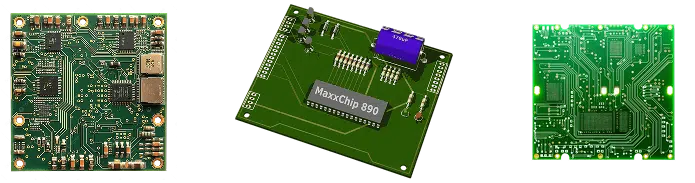
Our Custom FC PCB Assembly Service for Various Industrial Applications

FC PCB Assembly (Flip-Chip PCB Assembly) leverages four core advantages: "high-density interconnection, low parasitic parameters, high heat dissipation efficiency, and strong mechanical stability". It has become the "high-performance core carrier" for high-end electronic devices, covering key application scenarios from precision sensing to cutting-edge computing power.

FC PCB Assembly FAQs

We cooperate with multiple certification bodies and can handle CE certification, FCC certification, RoHS certification, FDA certification, etc.

We have a highly professional engineering team with extensive design experience in fields such as industrial control, consumer electronics, new energy, and medical devices.

Throughout the product development process, we confirm each step with the client. If the project design includes sample testing, we will conduct electrical performance testing, functional testing, performance testing, and reliability testing to ensure design quality.
Got any more questions?
Ultimate Guide 
to FC PCB Assembly

FC PCB Assembly Service

Various and Robust FC PCB Assembly Services
fc pcba
Prototype

Prototyping

From Gerber files to circuit boards, our professional engineering team provides you with the highest quality rigid PCB manufacturing services. We meticulously control every detail of the process, including drilling, electroplating, and AOI, ensuring precise control over trace spacing, thickness, and panel dimensions. We are committed to providing you with the most reliable PCB assembly.
  • Complete production line
  • Professional engineering support
  • 10+ years‘ manufacturing experience
fc pcb assembly
Production

Production

We have our own production lines and a robust manufacturing network. From PCB design, engineering, and manufacturing, we have sufficient capacity to provide you with professional and fast delivery services, whether for small or large batches. We spare no effort in providing consistent mass production services for your products.
  • Strong supply chain team
  • Competitive pricing
  • One-stop service from design to delivery

FC PCB Assembly
Service at Zintilon


How Does FC PCB Assembly Works

FC PCB Assembly (Flip-Chip PCB Assembly) mounts bare die face-down onto the PCB using gold/aluminum wire bonding or solder bumps, then under-fills and encapsulates — achieving “chip-level board packaging” with shortest interconnects.

1. Die Prep — wafer dicing, bumping (Au/Ni-Au/SAC)
2. Flip-Chip Bond — face-down bonding, ±5 µm precision
3. Under-fill — epoxy/silicone encapsulation, shear ≥80 MPa
4. Mixed Assembly — SMT control + FC high-density, thick-copper 4-20 oz
5. Test & Delivery — AOI + X-Ray + shear test, -55~125 ℃ verified

Let’s Build Something Great, Together